Thomas Keating Isolators allow UCSB Free Electron Laser to produce monochromatic high power pulses for Electron Spin Resonance
High Field Pulsed Electron spin resonance, with potential applications across a range of sciences - including molecular biology, require short (nanosecond time scale) monochromatic high power pulses of radiation in the mm-region of the Electromagnetic Spectrum.
Free electron Lasers have the potential to provide such pulses, but they do not produce, in their natural state, a monochromatic beam - many closely spaced frequencies are formed. However it is potentially possible to inject a low power signal into the laser cavity before it operates to "seed" the frequency, and stop other competing modes, at other frequencies, forming.
A solid state source - producing a few tens of milliwatts can provide such power, but such sources are themselves vulnerable to being destroyed by the very high power signal they have helped to form. Some form of isolation - a "non-reciprocal device" - is need to protect the source. Such a device will pass power in one direction with low loss but a power trying to move in the opposite direction will suffer highloss.
TK designed a double free space Quasi-optical ferrite isolator to protect a Virginia Diodes Inc 240 GHz source allowing the source to seed the UCSB Free Electron Laser, without being destroyed by the very high returning power UCSB colleagues wish it to produce - potentially pulses with power at the kW level.
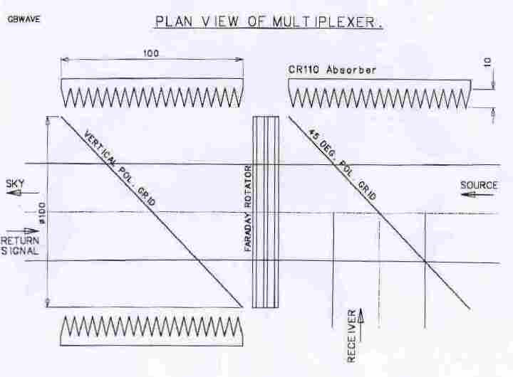
The principle of a free space isolator is quite simple: A linearly polarized wave passes unattenuated through a polarizing grid whose wires are set orthogonally to the beam's E field polarization. The beam enters a ferrite sheet whose magnetization is parallel to the direction of beam propagation, and normal to the surface of the sheet (reflections being minimised by the addition of an impedance matching or "blooming" layer). The polarization of the wave suffers Faraday rotation as it moves though the plate, and the thickness of the ferrite - about 2mm - is set such that a rotation of 45 degrees is achieved by the time the beam leaves the plate.
The beam then passes though a second grid, whose wires are set at 45 degrees to the initial polarization, also suffering negligible loss.
A returning beam which passes though this second grid suffers rotation in the same sense as the outgoing beam and finds itself with a polarization 90 degrees to in initial polarization and thereby reflected by that grid into an appropriate dump.
The figure below illustrates this process (though as drawn is part of a multiplexer/antenna feed looking at the sky, so the returning beam is recovered)
We have been working with TDK in Japan (H Taguchi-san and his colleagues) who have kindly provided us with Ferrite slabs with enhanced MM-properties - particularly in relation to their absorption losses.
Polarization diverse spectral transmission measurements have been made of these slabs in the 46 to 166 GHz range using Vector Network Analysers from both AB Millimetre and Agilent (The latter being
illustrated below)
The matching of the model to experimental results is strikingly good, as this plot of the model in black and the measured co-polar transmission in red shows

Ferrite slab transmission 46 to 166 GHz - AB measurements and model prediction
Taking the coefficients from this transmission information and using our Mathematica-encoded magnetodynamical model of the operation of the ferrite and the associated blooming layers - the image below gives isolation as a function of thickness and refractive index of such layers - TK determined the correct thicknesses of the Faraday rotator's layers. The coefficients forming the model are small in number: Just the scalar permeability, loss tangent and two frequencies associated with the internal field within the ferrite and magnetisation, respectively are needed.

However a single isolator (Polarizing wire grid; impedance matched ferrite sheet; polarizing wire grid) will not provide the isolation required, particularly at 240 GHz - a frequency above which most good isolators have hitherto been made. Two isolators were judged to be needed in series, to increase the isolation to well above 50dB: A one kW pulse would therefore only subject the "seeding" source to 10mW, and acceptable figure.

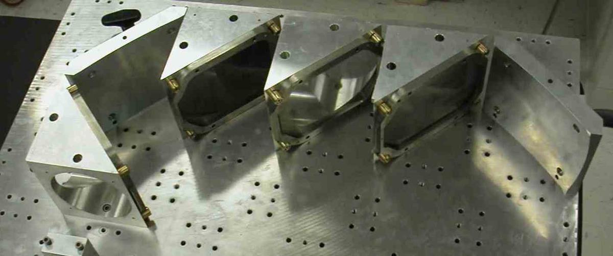
Pro/E CAD model of the Isolator. TK THz Absorber is added to the dump ports, to remove the unwanted power.
A section of the TK isolator, built out of our 125 mm Spilt Cubes, while undergoing tests at VDI, is shown below.
Measurements performed at VDI during the summer of 2006 showed insertion losses per isolator at the 1.8dB level and combined isolation at the 60dB level (such that 1 kW pulse would deliver only, say, 1mW to the diode in the final multiplier in the seeding source). During testing it was discovered that the cross-polar leakage, at around -45 to -50dB through the grid set between the two isolators was limiting the performance of the combined system. A second grid - not shown in the CAD model above, but visible in the photo below - was therefore added. The flexibility of our 125mm cube system allowed this
addition to be done simply and without difficulty.
In May 2007 came the news that the seeding process had worked, in an 19th May Email to his collaborators, Prof Mark Sherwin wrote
It worked with no tweaking, is now being optimized.
Susumu and Jerry are working on
characterizing it right now. When the FEL is turned
on with the 240 GHz injection (through the TK isolator),
the power spectrum of the FEL really does collapse
to a single mode that has at least 20 times more power
than any other mode, and has a Fourier-transform limited
linewidth of a few hundred kHz. Without injection locking,
the power is spread over roughly 2 dozen modes, with power
in each of those modes fluctuating greatly from pulse to pulse.
This has us all very excited (and relieved) since this is a critical
milestone on the path to pulsed EPR with the FEL."
The actual hardware, mounted in the FEL room is shown below
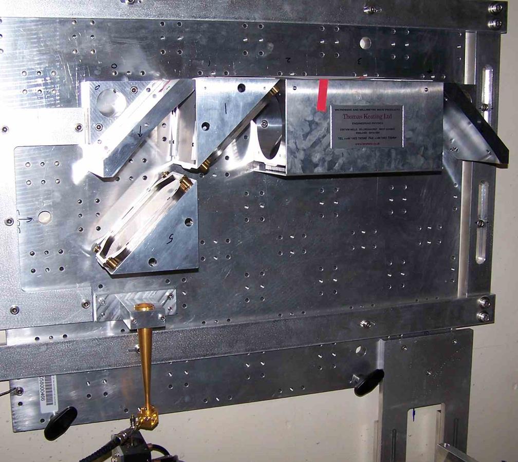
The VDI source is attached to the Corrugated feed horn on the lower left. The isolator section is covered in a metal sheet which holds TK Absorber.